Products are now more intelligent and connected than ever before but designing these products efficiently has not exactly been streamlined. With more competition in this space, and more complex tools required to create these products is an endeavor that requires precise coordination. Look at how Hawk Ridge Systems own engineers demonstrate how to seamlessly exchange PCB and mechanical design information.
Create Schematics and Printed Circuit Boards That Collaborates Seamlessly with Your Mechanical Designs
Video Transcript
Introduction
Good morning and good afternoon everyone. Welcome to the Weekly Wednesday Webinar series presented by Hawk Ridge Systems. Today’s topic is Seamless ECAD/MCAD integration with specifically SOLIDWORKS PCB. My name is Scott Davis, I’m the SOLIDWORKS PCB product manager here at Hawk Ridge Systems which includes two products.
We have our stand-alone SOLIDWORKS PCB fully integrated library development for schematic symbols and PCB footprints along with schematic editing capability for layout capability including the seamless integration. The secondary product is that very same seamless integration with SOLIDWORKS PCB connector exclusively for Altium Designer. So, for those of you in your organization that may be using Altium Designer, you can rest assured that the seamless integration that we’re going to demonstrate today works the same with Altium Designer.
Why SOLIDWORKS ECAD/MCAD?
So why use SOLIDWORKS ECAD/MCAD solutions? All of today’s products are typically highly mechatronic which is the new word for integrated electronics with mechanical enclosures, cases, rack mount systems, backplanes. You know, anything typically designed is going to have some mechanical enclosure and the challenges are, how do we fit our electronics into these mechanical enclosures to ensure that connectors are in the right places, mounting mechanisms are in the right places and we don’t have any clearance issues. Having a seamless integration between your PCB design and your mechanical enclosure assures that you can achieve these goals.
And we also give you full editing capabilities with SOLIDWORKS once you have collaborated your PCB design from a mechanical perspective, and we’ll demonstrate that today.
With the addition of our electronic design product, SOLIDWORKS PCB, the ecosystem now provides every solution for you during your product development cycles. Today we’re going to be focusing on the mechanical design and the electronic design with SOLIDWORKS PCB. We are using the version 2018 software, which includes many enhancements and some great features and moving forward.
Full Schematic Capture
As I mentioned earlier, SOLIDWORKS PCB is full schematic capture capability creating your electronic netlist, your part list, your bill of materials, all your component definitions, all your component parameters and then you associate that schematic to the layout tool which is going to provide you with full circuit board design capabilities. Again, along with all the necessary manufacturing output to create that bare PCB, and get that PCB assembled by your contractors.
Real-Time Collaboration
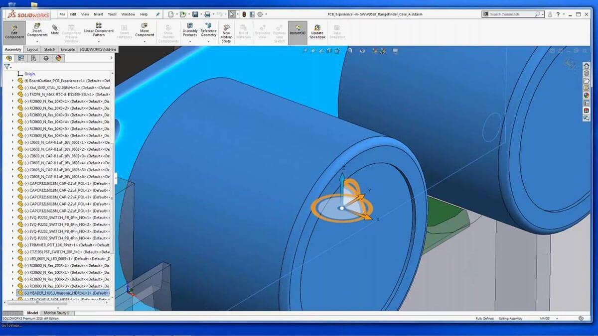
The product includes the real-time collaboration. It’s essentially pushing and pulling files to and from SOLIDWORKS. Once you are in the SOLIDWORKS environment, you’re going to have a three-dimensional model of your printed circuit board with editing capabilities for component placement, board outline adjustments, mounting hole mechanism adjustments and then you simply push that back to the SOLIDWORKS PCB tool, and you’ll visualize real updated edits.
Demonstrations
Today we’re working on two projects. We’re going to start with this Adreno board. It’s a multi-board project, so we’ll be working on the main board, then we’re going to collaborate that to SOLIDWORKS assembly and we’re going to make those assemblies together and we’ll adjust the rangefinder connector and I will show you how that automatically updates, inside of SOLIDWORKS PCB.
The second project is to utilize SOLIDWORKS to create the board outline, insert the slot, push that back to PCB so that we can add some simple mechanical components, and then we will load that into a new assembly and make some connector adjustments using SOLIDWORKS, and again, have that automatically update our PCB tool.
SOLIDWORKS PCB User Interface
This is the SOLIDWORKS PCB user interface. This is not new technology, and it is a very stable tool. It’s been on the market for quite some time. It does have a new user interface. It’s a more SOLIDWORKS inspired interface. It’s all TAB driven, and ribbon driven with simple icons that are easily found to execute the commands. All the editors within the tool are available, so we have our schematic editing tool which we would use to create individual schematic symbols. We also provide you with a symbol wizard, so you can quickly define your symbols and add them to your library, or you can copy symbols, modify those, and add those to your library. Library creation is extremely efficient. Library creation for footprints is also extremely efficient, and we give you the same type of wizard for footprint development that is based on IPC standards.
3D Model Tool
SOLIDWORKS PCB is a three-dimensional visualization layout tool. You can place your components in the three-dimensional model, simply by clicking the number two and number three we’re switching between our two-dimensional view and our three-dimensional view. The models that are embedded onto your SOLIDWORKS PCB footprints are the models that will directly collaborate to SOLIDWORKS. You have the capability to add SOLIDWORKS part models, step files, Parasolid files, or you can use the internal 3D model creation tools to develop your own models within the PCB tool.
Schematic Circuit
We’re going to first, quickly complete this schematic circuit because I want to show you how productive and how efficient the tool is to complete this circuit. Then we will associate that to the PCB, quickly place the components, do a little bit of trace routing just so you kind of get a feel for the functionality of the tool and the ease of use. But again, today’s focus is really this mechanical collaboration. How do I get this to and from SOLIDWORKS with accuracy and efficiency?
Let’s quickly get these parts on here and I’ll wire up the schematic, and then we’ll move into the layout. Parts are easily added from the library. You can simply drag and drop them from the library, or I can select the component and I can say, “Place component as well.” I am going to drag and drop a few of these and then I’ll use that other mechanism to add additional parts. With our part highlighted, we can simply just drag and drop these components onto our schematic.
Navigation
Let’s grab a couple capacitors here, get those placed and then we’ll finish that up with crystal and a few resistors. Navigation in the tool is extremely simple. You can zoom in and out with your control wheel, you can pan with the right mouse button. So again, very easy to navigate around and add components. I will place the resistor. Now, when I place the resistor, I’m going to get additional resistors on my cursor, and I can change those reference designators just by changing the text. Then, automatically by changing the text R3, R4 automatically comes to the cursor. We have all our components placed, now we need to wire up our schematic. Again, wiring is extremely easy. I can go to the home tab where most of the commonly used commands are going to be found, wire, place netlabel, power ports, if I need to add power ports, I have all these available to me. You can do harnessing hierarchal blocks, multi-channel, a lot of functionality in this schematic tool. Like I mentioned, it’s a complete standalone circuit board creation tool unto itself. But the value is the collaboration with SOLIDWORKS.
We’ll just go to the wire command, now we’re in the wire mode. When we highlight and hover over an active pin, our cursor turns red. I’ll just quickly get this, schematic wired up and then we’ll associate this to the PCB. Again, I’m continuing in the wire mode, SOLIDWORKS PCB is smart enough to know when I end connections and when I can move to a new connection.
We have multiple draw modes, I’m in the 90 degrees right now, but we can do a shift and I can do 45s, I can do full orthogonal, or I can do highlight where to. But typically, you route schematics in the 90-degree mode. You’re going to have those same modes when you route traces. With one additional mode, you’re going to be able to route art traces with the PCB tool. Just a couple more connections here, it will have this guy completely ready to go to our circuit board layout. Now, we have our circuit completed and we have a multi-sheet schematic here. So now, everything is already associated to our PCB which we’ll be working on here.
Import
Now, what I would do is just bring in those components. Let’s turn off that. We do an import. Now, on every import, you’re always going to get an engineering change order list. It’s describing to me what’s being added both from a component standpoint and from a wiring standpoint. We’re going to execute those changes, okay? Now, we’ve added all these components, we’ll move them over to the area where we can quickly place them and do some simple routing. By grabbing components and making them active on the cursor, this is where I would do rotations, and this is where I would flip the component from the top to the bottom.
That’s important because the surface at which the component is placed is the surface at which it represents in SOLIDWORKS. We’ll just quickly drop those in. Now, we’ll look at routing some of the traces and the capabilities there. You can see we have the guide wires here for the connections, and again, in the PCB tool, just like the schematic editing tool we saw, all the most common commands are going to be found on your home tab. You also have a view tab for viewing, zooming in, your project tab allows you to add multiple documents and add libraries, and import and export your design.
Autorouter
Additional tools are available. SOLIDWORKS PCB does contain an autorouter, so, you can quickly autoroute your PCB designs and set up your own autorouter stack or autorouter pass information, for those of you that have used autorouters before. You have a separate output tab for all your mechanical and manufacturing files (if you choose to have standalone mechanical files). But with the collaboration, we’re going to seamlessly send the file to SOLIDWORKS.
I go back to my Home tab and I do some route connections. Again, when I hover over active pins, you can see that the cursor puts a round circle and that tells me that’s an active pin.
I can bring this off and that the trace which looks fine for this component, but being a power trace, probably, going to want to make it a little bit larger. So, those wire modes I mentioned for a schematic, again, they’re the same in the PCB tool, there would be our arc routing mode. We would have 90 degrees, and then you have full orthogonal as well. It can be helpful when routing the shortest distance for printed circuit boards. We’ll go ahead and put in our first corner and will now switch this trace width to something doubled in size.
Now, the other feature of this tool is that if there’s a clear path to complete the route, which in this case, we have a clear path to the power pin of the battery, you can do a control left mouse button and it’ll finish the route for you. You don’t necessarily have to make all the clicks and end at the pin. If I do control left, it finished that route for me, that’s very handy and again, very efficient. Now our trace width remained at 20 because we set to 20, so we’ll drop it back to 10, then we’ll just route up this guy.
And again, control left key finishes that, we can bring this off, finish that, route some power traces and again, quickly and easily connect our circuit so that we can finish the design for manufacturing and prepare to go to SOLIDWORKS. So how do we get this design in SOLIDWORKS? I mentioned previously in the library that SOLIDWORKS is a three-dimensional visualization tool for PCBs and footprints. So again, by clicking the number three key, that’s our three-dimensional view of this design. This is what we would expect to see in SOLIDWORKS. I can absolutely move components and position them in the three-dimensional mode within SOLIDWORKS PCB.
Connector
SOLIDWORKS PCB includes what we call the connector. The operation of this functionality is driven by an installation of a database onto a network server. The SOLIDWORKS users with their username and login would connect to that database. SOLIDWORKS PCB users connect to that database, and now you can see here that we have simple push/pull buttons; one big advantage of this tool. SOLIDWORKS PCB can collaborate with as many SOLIDWORKS users that are within your organization. There is no licensing required at all for SOLIDWORKS 3D mechanical CAD.
Since 2016 Service Pack 3, that functionality is built into every version of SOLIDWORKS as an add-in, and you simply just turn it on, and then connect to the server.
Let’s push our board and tell our mechanical engineer that we’ve got, new PCB assembly. Now, the synchronization is based on the project name. Today we’re using PCB experience, the other project we saw on the slide will be projected A and we’ll come back, and we’ll demonstrate how to use SOLIDWORKS to create that outline.
SOLIDWORKS Add-ins
Let’s close PCB now and switch hats and become a mechanical engineer. We start with a blank SOLIDWORKS session. Under Tools, I mentioned earlier add-ins. Everyone has this capability now. You simply turn it on, it’s going to add a new icon over here for your SOLIDWORKS right-hand panel. By clicking that panel, you make your connection to the database and we do what’s called pull board.
Pulling Board
By pulling board, we’re looking in the database and we’re seeing multiple projects that we can now create SOLIDWORKS assemblies. We knew we’re working on PCB experience. I’ve got to save my file. And now SOLIDWORKS is going to create its normal SOLIDWORKS assembly structure. I’ve got the high-level project name and I’ve got subsequent SOLIDWORKS part models for all these components in a three-dimensional CAD tool. I have my board, and I have each individual component that I can move and edit in this assembly, but I can also take this assembly and I can load it into a higher-level assembly. That’s what we’re going to do today. We’re going to open another project which is the case, and the other previously collaborated baseboard.
Board to Board Connectors
Here’s our chassis with our baseboard. Now we can bring in our data card and associate these boards together. By simply using normal SOLIDWORKS commands, we can reference these two assemblies together to ensure that there’s proper fit. We just match up the mounting holes first. Now we have a board to board connectors. We take the back surface of our board and we say that we need that inserted into the surface of this connector.
But the manufacturer gives us the exact distance; 3.2 millimeters. With the 3.2-millimeter offset, you can see now that we have that assembly similar to the presentation slide. However, we’ve got a collision of the rangefinder into the chassis. We can use SOLIDWORKS evaluation tools and do an interference detection, and it will highlight this area. Now, it takes a little bit of time in some instances because we’re on the web and we’re doing a quick demonstration. I’m just going to go ahead and edit the assembly and modify that component.
Edit Mode
Now we’re in the edit mode for the main assembly. I highlight the component and I tell it that we need to move a triad. Because we just need to move it in the Y-dimension about- let’s go 2.4, roughly. All right. That’s close enough. So, again, we can do SOLIDWORKS tools to dimension it, center it, however, we like. We just visually centered it, now our rangefinder connector is perfectly positioned.
How do we get this back to the PCB tool in real time? And again, you can see we have created additional collisions. We can move these push buttons out of the way in SOLIDWORKS or we can certainly do that in the PCB tool as well because they’re already routed components. Now by opening this assembly, we can see we still have that same detection, our collision detection, and now by opening the connector panel again, we are pushing this information. As I mentioned before, you have a full project history of communication.
We now push this to the server and we say that we have moved H4. Now, if you’re working in an active assembly either in SOLIDWORKS or SOLIDWORKS PCB and you open the connector panel, the tool is smart enough to see that there’s new data and it will notify you automatically. Close this guy down, and we’ll come back for our second project. So back in the PCB tool, we can go to the 3D mode and we can open that connector panel, and there’s that notification; moved H4.
View Changes
We don’t do file import-export. We’re working on the real data. I mentioned that we give you visualization to see what’s going on, so by view changes, you can see that H4 was moved, and by clicking H4, I get animation showing me where H4 is moving. It’s all real time. We accept that change and instantaneously H4 moves, and then I go back to the two-dimensional view and see that I would have component movement clean up, trace routing to clean up, but once I finish that, I could go back to SOLIDWORKS in that same assembly and release my full mechanical assembled design. Collaboration allows you to collaborate multiple boards into one SOLIDWORKS assembly because as we know many products are multi-board products. So that was a simple connector movement.
Move Mechanical Components
Let’s look at our next project. How do I utilize SOLIDWORKS to create board outlines or move mechanical components? We’re going start with a blank circuit board. We have a simple five-connector schematic because the focus here is mechanical items. We’re going to utilize SOLIDWORKS to make sure that we’ve got these five connectors in the correct position. But first, we want to create the mechanical outline with SOLIDWORKS.
A feature of the tool is when you look at your circuit board layers stack-up, which defines your layers, your dialector thicknesses, you get an overall thickness. This board happens to be O62 or 62 mills. That’s a pretty common circuit board thickness along with 125 to mean there is definitely some industry commonality there.
Layer Stack-Up
SOLIDWORKS reads this thickness and creates the board exactly as you have defined in your layer stack-up so that’s an important feature. You’ll want to set that up first. We use the same process. Go to the view tab, open our connector panel and we’re going to tell SOLIDWORKS that we have a new board, and we’ll simply post that up. We’ll switch back to SOLIDWORKS again so that your mechanical engineering counterparts would know, you can send them a quick message, but as soon as you start collaborating multiple assemblies or multiple iterations, that communication’s going to be automatic. But for the very first pole, you must let them know that “Hey, I just put a new design on the database.”
Chassis
It’s the same process. Pull board, there’s our list of projects. Now, we’re working with PCB project A. Let’s save that assembly. There’s our blank board. Again, the O62 or 62 mil thickness, that’s the only dimension that is on that sketch inside of SOLIDWORKS. From here, I’m going to insert my chassis component. Now, this chassis, it’s not completely designed, but my goal is to use the bottom surface that I have defined as my board outline and include the sketch. When I iterate the second time, I’m going to utilize a newer updated, modified chassis, but I can still reference it to the features of the PCB and match that up to my new chassis.
Board with Slots
Let’s reference these two parts together. Now we’re able to slide obviously the chassis anywhere we like on the surface of the PCB and we won’t lose that reference. By dropping that down, we’re good. Now we just simply need to edit the board sketch. You can delete the perimeter because we’re going to use this inside surface and we’re going to make that the board. Now in two clicks, we’ve got a board with slots. We’re going to put the cutout in. We’ve got arcs, we’ve got angles. I don’t care which PCB tool you’re using today, this is not an easy board outline to draw inside of a PCB tool. Now, you may be able to convert a DXF and other items like that, but how do you ensure the accuracy? By using SOLIDWORKS to create the board, we know it’s 100% accurate.
SLOT
Let’s edit this part, and sketch in that slot. All right we convert that, now we simply use SOLIDWORKS extruded cut feature and we cut away all the material. Do a quick rebuild, go back to our assembly full model. Now we have our slot that matches what we developed in SOLIDWORKS. Let’s get those other remaining components onto the board and bring this back to that updated chassis for the next level assembly. So again, we just push, and again, there’s that comment; add a new board and all the history.
We adjusted the outline, but I need the PCB designer to add some mounting holes so that when I bring the board back in, I can position those mounting holes on to my updated chassis standoffs. Now add 3.1 MTGs. My PCB designer is going to see that note the real-time and add those PCB holes for me. Right, back in the PCB, we could have been doing things like additional schematics or even, you know, some routing if the components were there, anything that wasn’t affected by the board outline or the slot location.
CAD Panel
Open our CAD panel, there’s my note that says adjusted the outline and I need to add those three holes. Let’s look at the visualization again, there’s the new outline, here’s the slot, now, this happens to be the chassis. You can send SOLIDWORKS parts that you add to the assembly. You can send those back to the PCB and you can pick and choose whether to bring those into your circuit board design.
In this case, I’m not going to bring the chassis in at this time, because it’s not the final one, but by doing a right click “check all”, I can then just turn off that chassis. With one click, instantaneously again, there’s my new outline with my slot created by SOLIDWORKS.
Import Changes
So now we can go back and import the changes, again. There’s our ECO adding five parts. Let’s get these parts on the work surface and push this back to SOLIDWORKS so that we can check the verification of placement and adjust if necessary. And there was that note to add three mounting holes. On the Home tab I would add pad, check my pad parameters, hole size needs to be 100. We don’t care where we put them in PCB, we didn’t get any dimensions and we weren’t instructed where to place them because we don’t care, we’ll let SOLIDWORKS handle that.
We added the parts, we added the holes, and have a quick three-dimensional view. That’s probably what our SOLIDWORKS model’s probably going to look like. We can go now push this to SOLIDWORKS, and we can say that we’ve added the parts and the MTGs. All right, so let’s get into SOLIDWORKS now, in the meantime I mentioned I’ve created a new modified chassis. My surface bottom’s still the same pattern because I knew that’s what I wanted initially. I’m going to create a new assembly again using that same project, just overwrite my other file.
Now, this assembly tree and some of you may be used to using step files and other methods to get your circuit boards into SolidWorks, but by using the collaboration, you now have a much more intelligent assembly tree, right? I’ve got each component, and it’s telling me the reference designator for each of those components, okay? So now I’m going to add my new chassis, and we’ll match that up and do some checking for interference. Again, we’re going to take the surface of our standoff. And that needs to be referenced on the back of the PCB. Now what we can do is we can reference the slot faces together to ensure that we have that relationship correct.
New Board
Again, with a simple four clicks in SOLIDWORKS, I’ve now got that new board updated chassis, and now I’ve sent that board to chassis clearance and I’ve added a slot for the power connectors and my audio connectors. Let’s do that evaluation of our interference with SOLIDWORKS tools.
When we calculate that, right? SOLIDWORKS immediately tells me, “Hey, you got a power pin going right through your chassis, that’s not going to work.” Let’s just move the component in SOLIDWORKS and have that automatically update the PCB. Again, I can do this dimensionally, visually, reference, however, I like. I’ll just do it visually for ease of time. So, again, I can now update my PCB with that, but before I do that, I need to move these mounting holes to match my standoffs.
Move Mounting Holes
So inside of the board part, right? The separation between all through holes and models occurs, so all the holes are now part of the board part, but the models remain individual SOLIDWORKS parts. We just simply edit this sketch. We can change our view to the wire mode. Now in SOLIDWORKS I can drag and drop this anywhere I want. I could create dimensions. I can also change its diameter. If I change that whole diameter in SOLIDWORKS, it will absolutely update the drill value in the PCB tool, because your PCB vendor is going to go off of your, NC drill file to drill the board obviously, so there is a direct correlation between the diameter and SOLIDWORKS and your drill size value in the PCB tool.
Let’s just drop these other two together, and then we’ll push this back. Now, in doing so, I can also do some experiments. My PCB designer can look at some suggestions I might have mechanically because we give you the view and accept-reject capabilities. You don’t have to make changes, you can absolutely reject them. I want to look at moving audio connectors up into this area. Maybe I could shave chassis material. Maybe I could save some PCB material, so I would push this back now and say that we moved the power, and the MTGs, and review audio placement.
Again, there’s all my history, I post this. Now, we’re going to continue in this assembly but, this we’re not going to close it down. In SOLIDWORKS PCB, by opening the panel, now I get a whole list of changes. With animation, we can see where every mounting hole and every connector’s going, so I can see that the power connector looks okay, but I don’t know really what’s going on with these audio jacks. He said, “Review that.” So, I’ve reviewed it as the electrical engineer, and said, “Absolutely not,” because I have plans to put magnetics, or additional power circuits, or maybe digital circuits up in that area, so, we’re not going to be able to take a look at that today. But we can look at the movement of the mounting holes. Now, if you had routed connections to any of these connectors and you move them in SOLIDWORKS, it will not jeopardize the integrity of the electrical connection. It’ll just create a new guide wire like we saw in the first project. It’ll create a new guide wire from the end of the route to the location of the new pin.
We’re going to go ahead and accept everything. We’re not bringing the chassis in again. We’re not going to move J4 and J3 because those were the audio connectors.
Final Assembly
Now accept that. I would go ahead and finish my board, do all the routing, do all the documentation, and then always, as the final iteration, I would collaborate this to SOLIDWORKS to get that final assembly. That can also allow you to release your mechanical assemblies including your electronic assemblies with bills and materials, with documentation, side views, front views, all that is capable inside of SOLIDWORKS now that you’re sending real data.
So, we’ll push this back and we’ll just say that we’ve got this is the final PCB. All right. Now, we give you that same animation inside of SOLIDWORKS, so, you can see what’s being moved here is that J3 and 4, they’re going back to their original location. Now, it’s not going to bring in the reference board because it’s the chassis, it’s already in my SOLIDWORKS assembly, that’s why the color of the box is pink. So, I am going to accept the changes to move the audio connectors back to their original location. Rebuilds the part and rebuilds the assembly.
That’s how you perform seamless integration between a circuit board design tool SOLIDWORKS PCB and SOLIDWORKS 3D mechanical. If you’re interested in some additional support for creating Schematics and Printed Circuit Board Layouts or additional questions on SOLIDWORKS PCB, please CONTACT US today!